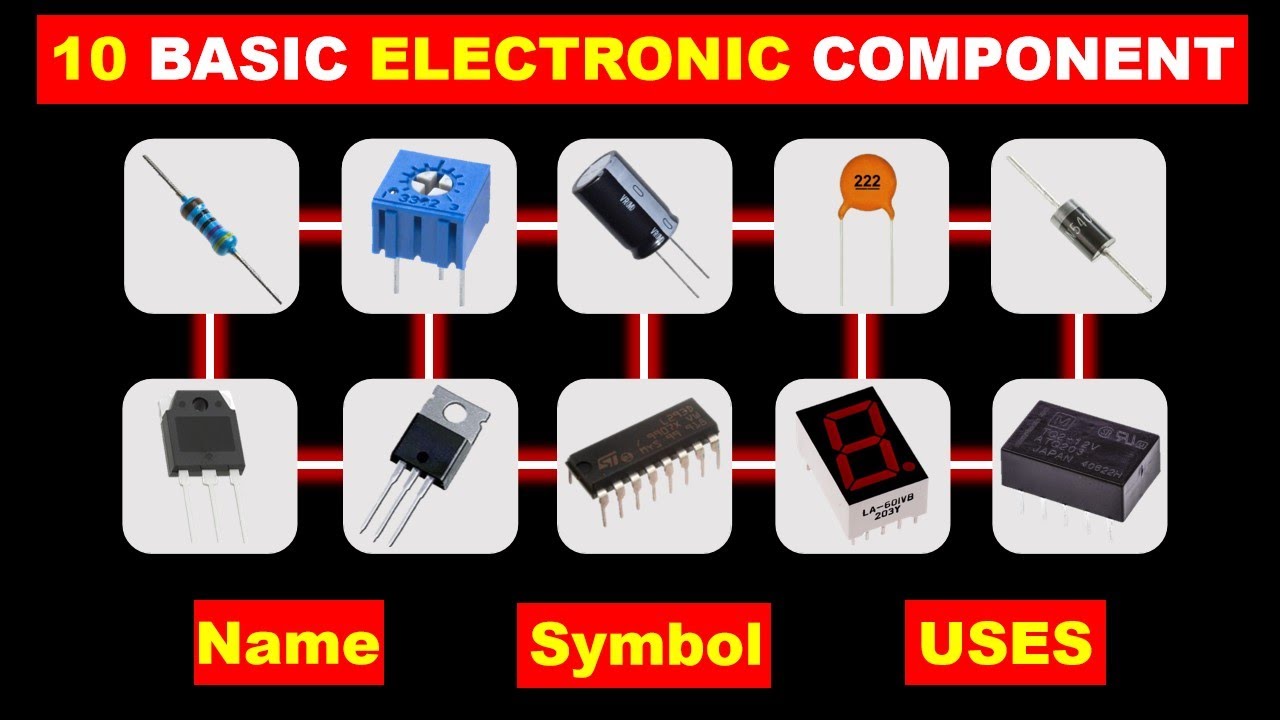
Transistors Explained - How transistors work
TLDRThe video script delves into the intricacies of transistors, highlighting their critical role in electronics as both switches and amplifiers. It distinguishes between bipolar and field-effect transistors, with a focus on the bipolar type. The script explains the function of the emitter, base, and collector, and emphasizes the importance of referring to the manufacturer's datasheet for specifications. It illustrates the automation capabilities of transistors in controlling circuits and amplifying signals, using relatable examples like lighting a bulb and connecting to a microphone. The explanation extends to the working principles of NPN and PNP transistors, the concept of doping in semiconductors, and the formation of PN junctions. The analogy of water flow through pipes aids in understanding the functioning of transistors, making complex concepts accessible.
Takeaways
- 📱 Transistors are fundamental electronic components with the ability to act as switches and amplify signals.
- 🔧 There are two main types of transistors: bipolar and field-effect, with the video focusing on the bipolar type.
- 🔌 Transistors have three pins labeled E, B, and C, representing the emitter, base, and collector respectively.
- 💡 The base pin controls the flow of current in the main circuit, allowing for the transistor to act as a switch.
- 🌡️ Higher power transistors often have a metal case and are attached to heat sinks to dissipate heat generated during operation.
- 🔍 The part number on the transistor's body is essential for referencing the manufacturer's datasheet for specifications.
- 🔌 In a circuit, a small voltage applied to the base pin can control a larger voltage and current in the main circuit, demonstrating the transistor's amplifying ability.
- 🔄 The current gain (beta) is the ratio of collector current to base current and is a crucial parameter detailed in the datasheet.
- 🔴 NPN and PNP are the two types of bipolar transistors, differing in the direction of current flow and the configuration of their layers.
- 🌊 The video uses an analogy of water flowing through pipes with a gate to explain the functioning of an NPN transistor.
- 🔋 Understanding the difference between conventional current flow and actual electron flow is vital for proper circuit design and analysis.
Q & A
What is the significance of transistors in the field of electronics?
-Transistors are extremely important in electronics as they can act as switches to control circuits and also amplify signals. They are fundamental components in modern electronic devices and have revolutionized the electronics industry due to their ability to control large currents with small inputs and their amplification capabilities.
What are the two main types of transistors mentioned in the script?
-The two main types of transistors mentioned are bipolar transistors and field-effect transistors. The script primarily focuses on the bipolar version.
How do low power and high power transistors differ in terms of casing?
-Low power transistors are enclosed in a plastic case for protection, while high power transistors have a partly metal case to help dissipate the heat generated, which can damage the components over time. High power transistors are usually attached to a heat sink for efficient heat removal.
What information can be found on the body of a transistor?
-On the body of a transistor, there is text that indicates the part number, which can be used to find the manufacturer's datasheet with detailed specifications and ratings for the transistor.
How do you identify the pins of a typical NPN transistor?
-In a typical NPN transistor with a flat edge, the left side is the emitter, the middle is the base, and the right side is the collector. However, it's important to check the manufacturer's datasheet as not all transistors follow this configuration.
How does a transistor act as a switch in a circuit?
-A transistor acts as a switch by blocking the flow of current when no voltage is applied to the base. When a small voltage is applied to the base, it allows current to flow in the main circuit, effectively turning on the transistor and the circuit.
What is the role of the base pin in controlling the transistor?
-The base pin controls the transistor by receiving a small voltage that influences whether the transistor allows current to flow in the main circuit. A minimum voltage, typically around 0.6V to 0.7V, is needed for the transistor to turn on.
How does a transistor function as an amplifier?
-A transistor functions as an amplifier by using a small input signal at the base pin to control a larger current in the main circuit. The change in voltage at the base pin results in a larger change in the main circuit, effectively amplifying the input signal.
What is the current gain of a transistor and how is it calculated?
-The current gain, denoted by beta (β), is the ratio of the collector current to the base current. It can be calculated by dividing the collector current by the base current. This ratio is provided in the manufacturer's datasheet.
How do NPN and PNP transistors differ in terms of current flow?
-In an NPN transistor, the current combines, with electrons flowing from the emitter to the base and out of the collector. In a PNP transistor, the current divides, with some of it flowing into the base and the rest out of the emitter and through the collector.
What is the significance of the depletion region in a PN junction?
-The depletion region in a PN junction is where excess electrons from the N side move over to occupy holes in the P side, creating a barrier with a build-up of electrons and holes on opposite sides. This region is crucial for the functioning of the transistor as it forms an electric field that prevents more electrons from moving across, thus controlling the flow of current.
How does doping silicon change its electrical properties?
-Doping silicon with a material like phosphorus (N type doping) adds extra electrons, making it more conductive. Doping with a material like aluminum (P type doping) creates holes by having fewer electrons available for sharing, which also alters the electrical properties and allows for the creation of PN junctions, essential for transistor function.
Outlines
📡 Introduction to Transistors and Their Functions
This paragraph introduces transistors as one of the most significant inventions in electronics, highlighting their versatility in shape and type, with a focus on bipolar transistors. Transistors serve dual roles: as switches to control circuits and as amplifiers to boost signals. The physical construction varies from low power transistors in resin cases to high power ones with metal casings attached to heat sinks for cooling. The paragraph also delves into the identification of transistors through part numbers and datasheets, explaining the significance of voltage and current ratings. The anatomy of a transistor is discussed, with pins labeled E, B, and C for emitter, base, and collector, respectively. The explanation includes how these components work in a circuit, with the base pin controlling the flow of current through the main circuit, exemplified by a light bulb analogy. The paragraph concludes with the concept of using transistors for automation and remote control, emphasizing the need for a minimum voltage for the transistor to function effectively.
🔄 Understanding Bipolar Transistor Types and Current Dynamics
This section delves into the two primary types of bipolar transistors, NPN and PNP, explaining their physical similarities and the necessity of checking part numbers for differentiation. It describes how current flows through these transistors when connected to a battery and a switch, using a simplified model to illustrate the flow of current in both types. The paragraph further explains the combination of current in the NPN transistor and the division in the PNP transistor, providing specific values for each type. It also introduces the electrical symbols for transistors and the conventional current direction used in circuit design. A metaphor of water flowing through pipes with a gate is used to analogize the functioning of an NPN transistor. The paragraph touches on the historical discovery of electron flow by Joseph Thompson and the difference between conventional current theory and actual electron flow. It also briefly discusses the role of conductors and insulators in electronic circuits.
💡 The Physics of Semiconductors and Doping
This paragraph explores the atomic structure of metals and insulators, focusing on the behavior of electrons in different materials. It explains the concept of valence and conduction bands and how they relate to the conduction of electricity in materials like copper (a conductor) and rubber (an insulator). The paragraph then introduces semiconductors, such as silicon, which can act both as an insulator and a conductor when doped with specific materials to form P type and N type materials. The process of creating a PN junction by combining these doped materials is described, along with the formation of a depletion region and the resulting electric field. The dynamics of voltage application and the resulting forward and reverse biases are explained, detailing the movement of electrons and the creation of an electric field that prevents further electron movement. The paragraph also discusses the doping process in more detail, illustrating how the addition of phosphorus and aluminum changes the electrical properties of silicon, leading to the formation of NPN and PNP transistors.
🔧 Operation of NPN Transistors and Biasing
The final paragraph focuses on the operation of NPN transistors, detailing the structure with two N type layers and one P type layer. It explains the concept of barriers and how they prevent current flow under normal conditions. The paragraph describes the process of creating a forward bias by connecting a battery across the base and emitter, leading to the collapse of the barrier and the movement of electrons. The role of doping in the transistor's function is emphasized, with the heavily doped emitter releasing excess electrons and the lightly doped base allowing few electrons to occupy holes. The paragraph also explains the reverse bias scenario and how it affects electron and hole movement. The impact of varying voltage on the base pin and its effect on transistor operation is discussed, with a higher voltage leading to increased current and electron movement. The summary includes an overview of the electron flow in the emitter and collector sides of the transistor and concludes with a call to action for further learning in electronic engineering.
Mindmap
Keywords
💡Transistor
💡Bipolar Transistor
💡Field Effect Transistor (FET)
💡Amplifier
💡Heat Sink
💡Current Gain (Beta)
💡PNP and NPN Transistors
💡Doping
💡Emitter, Base, Collector
💡Forward Bias and Reverse Bias
💡Datasheet
💡Electronic Circuits
Highlights
Transistors are among the most important electronic devices ever invented, with the ability to act as switches and amplify signals.
There are two main types of transistors: bipolar and field effect, with the video focusing primarily on the bipolar type.
Transistors come in various shapes and sizes, and their external casing can range from resin to metal, depending on power requirements.
Low power transistors can operate without a heat sink, while higher power transistors require attachment to a heat sink to manage heat dissipation.
The part number on the transistor's body is crucial for referencing the manufacturer's datasheet, which provides voltage and current handling specifications.
Transistors have three pins labeled E, B, and C, representing the emitter, base, and collector, respectively, with their functions and connections varying by type.
The base pin controls the transistor's behavior, allowing small changes in voltage or current to manage larger currents in the main circuit.
A transistor can be turned on by applying at least 0.6V to 0.7 volts to the base pin, with changes in voltage affecting the main circuit significantly.
The current gain, symbolized by beta, is the ratio of collector current to base current, and can be found in the transistor's datasheet.
NPN and PNP are the two main types of bipolar transistors, with their operation differing in terms of current flow direction and connections to the battery.
In an NPN transistor, the current combines, while in a PNP transistor, the current divides, with different flow patterns and behaviors.
Transistors are represented on electrical diagrams with specific symbols, with the arrow on the emitter indicating the direction of conventional current flow.
The functioning of a transistor can be likened to water flowing through pipes with a gate, where the gate controls the amount of water allowed to flow.
Electrons actually flow from negative to positive in a circuit, contrary to the conventional current assumption, with their movement being fundamental to the operation of semiconductors.
The valence shell and conduction band of a metal conductor like copper overlap, allowing easy electron flow, while in an insulator, these bands are distinct, preventing electron flow.
Semiconductors like silicon can be doped with materials to change their electrical properties, forming the basis for PN junctions and transistor construction.
The PN junction is formed by combining N type and P type doped silicon, creating a depletion region with a potential difference that can be manipulated for electronic control.
In NPN transistors, a forward bias at the base-emitter junction allows electrons to cross the barrier, while a reverse bias at the collector-emitter junction controls the flow of electrons in the main circuit.
The video concludes with an encouragement to continue learning about electronics engineering and a reminder to follow the channel on various social media platforms.
Transcripts
Browse More Related Video


5.0 / 5 (0 votes)
Thanks for rating: